
Course 037 Power Semiconductor Device Technology
Available course dates
This course has no planned course dates.
If you are interested in this course, contact us at cei@cei.se
037 Power Semiconductor Device Technology
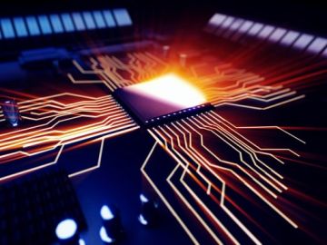
TECHNOLOGY FOCUS
The rapid growth of the semiconductor industry has relied on the continual evolution of materials and processing compatible with fabricating modern silicon-based integrated circuits. Power semiconductor devices do benefit from scaling, but most of the performance improvements come from wafer fab and assembly process innovations, such as vertical gates, backside thinning, and Direct Bonded Copper (DBC) substrates, and from new substrate materials, such as SiC and GaN.
COURSE CONTENT
This course includes all the key materials involved and the process areas utilized in device manufacturing, including the starting wafers, device design, wafer fab processes, assembly processes, yield, and reliability. The course is addressed to a broad audience and is not intended as a research review, although it will be taught at a high level and in many areas will require familiarity with the subject matter.
WHO SHOULD ATTEND
The course is addressed to a broad audience and is not intended as a research review, although it will be taught at a high level and in many areas will require familiarity with the subject matter.
Daily Schedule
1. Introduction; Day 1 AM.
This section provides a brief overview of power semiconductor applications and the basics of power conversion, including the challenges associated with power conversion.
a. Application
b. DC-to-DC conversion
c. AC-to-DC conversion
d. DC-to-AC conversion
2. Brief Review of CMOS Device Physics; Day 1 AM.
This section provides a review of types of devices used for power electronics.
a. p-n Junctions
b. Bipolar Transistors
c. MOS devices
d. MOSFET devices
e. HEMT devices
3. Wafer fabrication ; Day 1 PM.
This section is a review of wafer fabrication processes and challenges, especially with regard to defects in each type of substrate.
a. Si wafers + epitaxy
b. SiC wafers + epitaxy
c. GaN wafers + epitaxy
4. Basic Semiconductor processes; Day 1 PM.
This section provides an overview of semiconductor process technology with the main focus on Si devices, but with additional discussion on unique processes for SiC and GaN.
a. Lithography
b. Etch
c. Isolation
d. Gate Dielectrics
e. Gate Stack
f. Ion Implantation
g. Contacts
h. Interconnects.
i. Packaging
5. Power Semiconductor Devices. Day 2.
This section is a detailed discussion on device design and fabrication.
a. Si
i. Rectifiers
ii. MOSFETs
iii. IGBTs
iv. Thyristors
v. Bipolar-CMOS-DMOS (BCD)
b. SiC
i. Rectifiers
ii. MOSFETs
c. GaN
i. Accumulation mode
ii. Depletion mode
6.Yield. Day 3.
This section is a brief review of in-line process monitoring and test strategy for power devices.
a. Yield loss mechanisms
b. In-line monitoring
c. Statistical Process Control
d. Test strategy
7. FEOL Reliability;
This section reviews reliability requirements and qualification of power devices.
a. Reliability statistics
b. JEDEC and AEC1010
c. Gate oxide Breakdown
d. Bias Temperature Instability (BTI)
e. High Temperature Reverse Bias (HTRB)
f. Hot carrier instability (HCI)
g. Unclamped Inductive Switching (UIS)
h. Avalanche Stress Test
i. Safe Operating Area (SOA)
j. Latchup
k. Electrostatic Discharge (ESD) and Electrical Overstress (EOS)
l. Soft Errors
8. BEOL reliability;
This section reviews reliability requirements and qualification of interconnects and packaging for power devices.
a. Electromigration
b. Stress Migration
c. TDDB
d. Package reliability
i. Moisture Sensitivity Level (MSL)
ii. High temperature storage
iii. Thermal cycle
iv. Power-Temperature cycle (PTC)
v. Highly Accelerated Stress Test (HAST)
vi. High Temperature Operation Life (HTOL)
vii. Early Life Failure Rate (ELFR)
9. Future directions.
This section describes industry trends and outlook for the future.
a. Si Devices
b. Compound Semiconductors.
c. 3D integration.
ALL COURSE DATES FOR THE CATEGORY: Semiconductors Technology
099 Integrated Circuit and MEMS Fabrication Technologies
Designed to bridge the gap between device physics and electronic characteristics, the course examines the intricate process flows of CMOS manufacturing and MEMS fabrication, highlighting how these technologies are integrated in real-world applications. A detailed discussion of 3D micromachining techniques further reveals the power of MEMS in creating multifunctional microsystems.
What You’ll Learn
-
The basic physical principles of microelectronic devices
-
Key IC fabrication technologies and how they shape device behavior
-
Silicon bulk and surface micromachining for MEMS fabrication
-
Complete CMOS process flow and technology integration challenges
-
The evolution and ecosystem of modern microfabrication